LED Production
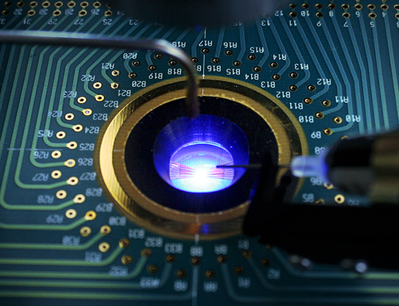
Complete characterization of LED chips on the wafer

Precise measurement of the smallest deviations ensures accurate binning of LEDs
Today, conventional light sources have largely been replaced by LED-based light sources. In many cases multiple LEDs are installed, and as far as possible they are required to exhibit the same behavior, optically as well as electrically.
Because the properties of these semiconductor components depend, among other things, on precise setup of the layer structures and their composition, tiny deviations in the individual LEDs can have a serious impact on the optical and electrical properties of the individual LEDs. Each and every LED must be precisely characterized and subdivided into groups (bins). Depending on the manufacturer, LEDs are often subjected to several tests during their production process. This normally takes place at wafer level (wafer probing and sorting) and on the finished, saleable LED.
The challenge in LED in-process inspection
In production environments, exacting requirements are placed on measuring systems:
- - High degree of reliability in 24/7 use
- - Short measuring times, to achieve a high throughput
- - Precise, controlled timing of measurements (triggering)
- - High reproducibility of the results from system to system
- - Measurement adapters specially tuned to the production process

